P-type SiC substrate materials are mainly used for homoepitaxy and the fabrication of ultrahighvoltage powersemiconductor devices.
They are widely applied in smart grids represented by ultrahighvoltage power transmission,
as well as in rail transit and industrial highpower power supply fields.
*Please contact our sales for more detailed information.
>Contact us
Specifications
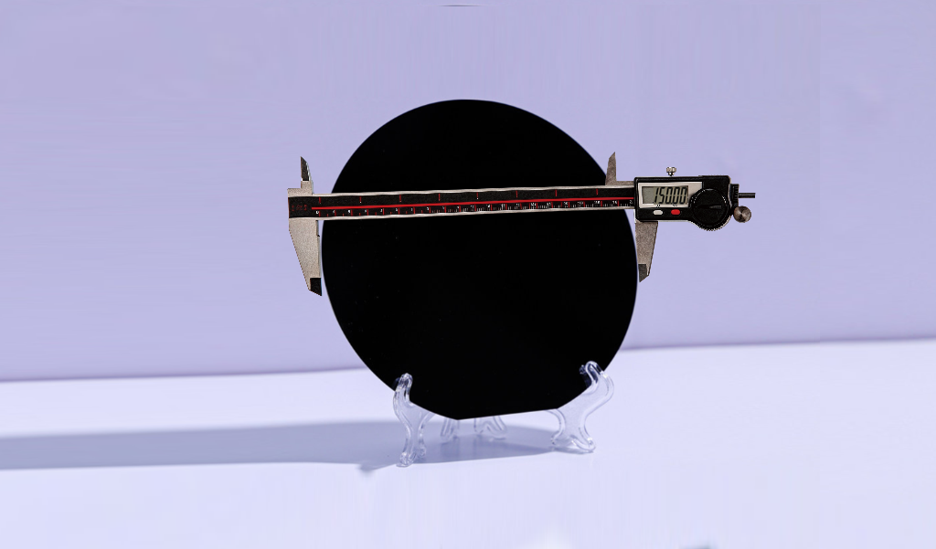
6-inch
-
Diameter 150.0mm+0mm/-0.2mm
-
Surface Orientation 4°toward<1120>±0.5°
-
Primary Flat Length 47.5mm±1.5mm
-
Primary Flat Orientation <1120>±5.0°
-
Notch Orientation /
-
Notch Angle /
-
Notch Depth /
-
Thickness 350.0um±25.0um
-
Polytype 4H
-
Type p-type
*Please contact our sales for more detailed information.
>Contact us
Specifications
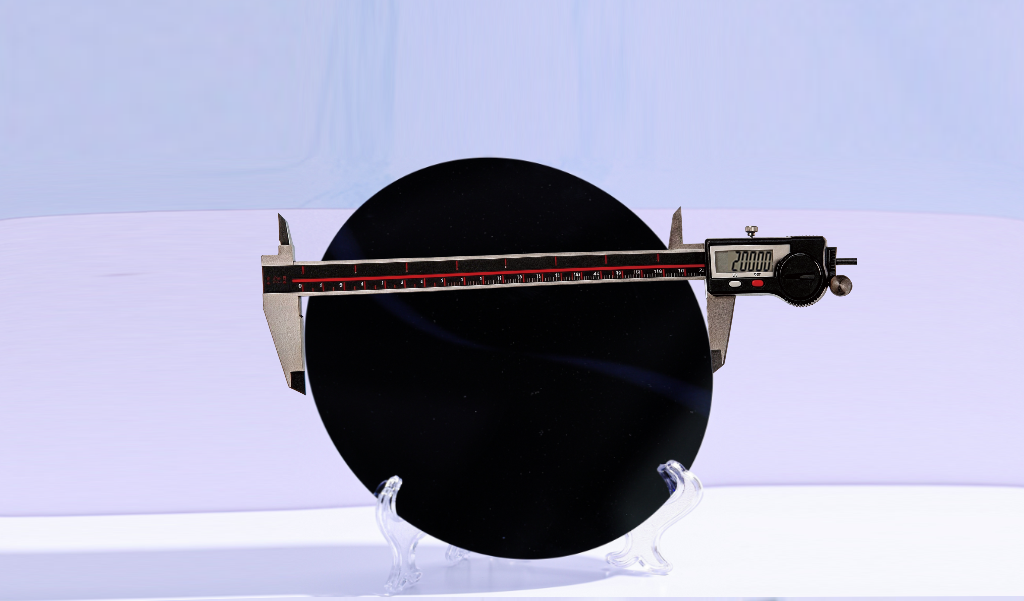
8-inch
-
Diameter 200.0mm+0mm/-0.2mm
-
Surface Orientation 4°toward<1120>±0.5°
-
Primary Flat Length Notch
-
Primary Flat Orientation /
-
Notch Orientation <1100>±1.0°
-
Notch Angle 90°+5°/-1°
-
Notch Depth 1.0mm+0.25mm/-0mm
-
Thickness 350.0um±25.0um
-
Polytype 4H
-
Type p-type
*Please contact our sales for more detailed information.
>Contact us
Specifications
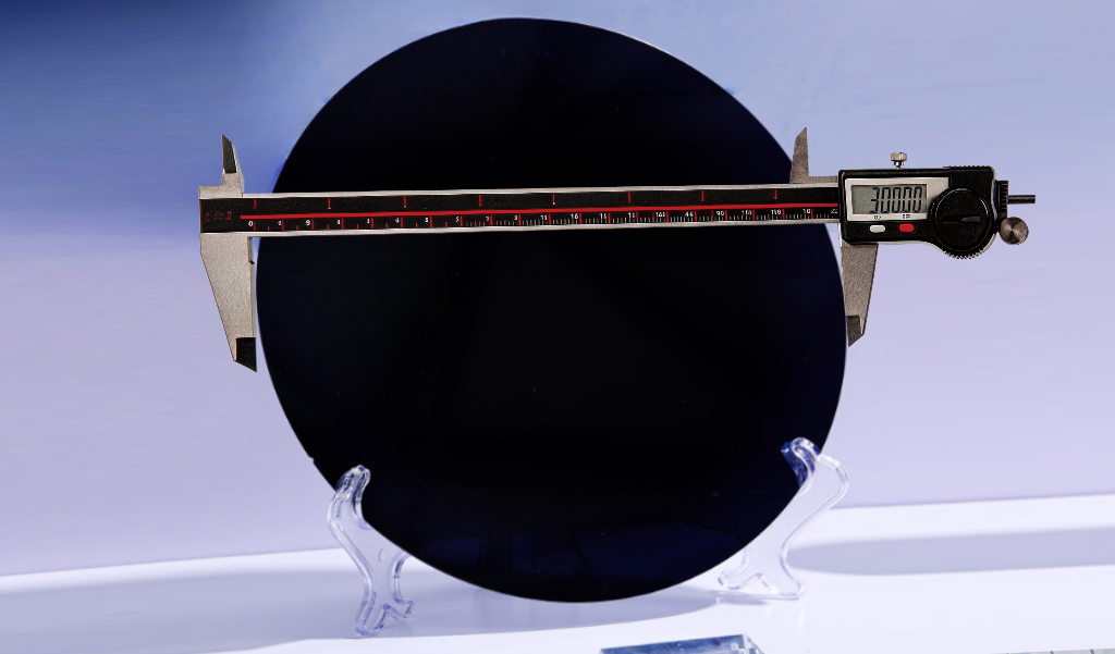
12-inch
-
Diameter 300.0mm±0.5mm
-
Surface Orientation 4°toward<1120>±0.5°
-
Primary Flat Length Notch
-
Primary Flat Orientation /
-
Notch Orientation <1100>±5.0°
-
Notch Angle 90°+5°/-1°
-
Notch Depth 1.0mm+0.25mm/-0mm
-
Thickness 750.0um±25.0um
-
Polytype 4H
-
Type p-type